32,768 compute units.
One deterministic fabric.
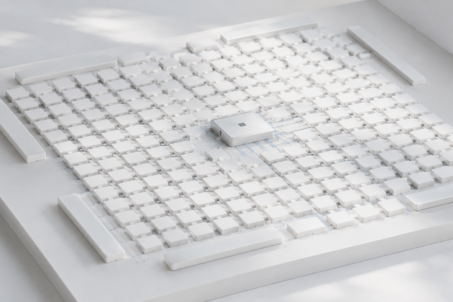
The Morphific Processing Unit (MPU) is a state-resident structural computing array. 32,768 Compute Units arranged as a 256 × 128 grid, operating on 16-bit FP16 data paths at 1 GHz — with scheduling fixed at compile time, not runtime.

Why this matters
Each Compute Unit contains a small instruction cache, register file, processing element, and writeback path — all on a 16-bit FP16 datapath. Every CU runs independently addressable instructions. There is no data cache, no cache coherence, and no runtime memory management.
The architecture operates in four deterministic phases — LOAD (weights ingress from DDR7), EXECUTE (computation on the PE array), READOUT (structured result readback), and RELOAD (phase-swap for multi-layer models). No memory-to-memory traffic exists. Results travel by wire, not through memory.
The interconnect identity
The entire fabric design derives from one identity:
One row stream equals exactly one SerDes lane. The fabric lane rate is derived from the compute rate by construction — not an independent assumption. This is why the interconnect can be lean: the PHY and the compute are matched.
Physical design parameters
| Process Node | TSMC N7 | ~76 MTr/mm², logic + SRAM mix |
| Die Dimensions | ~20.5 × 21.0 mm | 84 mm perimeter, within reticle limit |
| Clock Frequency | 1 GHz | 0.5 mm wire length per cycle |
| CU Array | 256 cols × 128 rows | Central ~85% of die area |
| On-Chip SRAM | 384 MB total | 12 KB I-SRAM × 32,768 CUs |
| Operator Latency | MAC/×/+/= 1 cycle | Divide = 4 cycles; exp = 50 cycles |
| External Memory | 4× GDDR7 | ~192 GB/s/chip raw bandwidth |
| TDP | ~250–350 W | ~60–80 W/cm², standard cold plate |
| SerDes Lanes | 256 per chip | 16 Gbps/lane NRZ (= 16-bit FP16 @ 1 GHz) |
| Pins | ~4,000 | ~1,000 signal + ~3,000 P/G (3:1 ratio) |
| V-EXT Port | 16 lanes | 32 GB/s for inter-domain rail links |
Four-phase operation
The architecture operates in four deterministic phases with no memory-to-memory traffic.
Weights and state ingress from DDR7 via CSL into column structure.
Computation on the PE array. Results travel by wire, not through memory.
Structured readout of computed results back to the system.
Phase-swap via dual-bank atomic switch for multi-layer models.
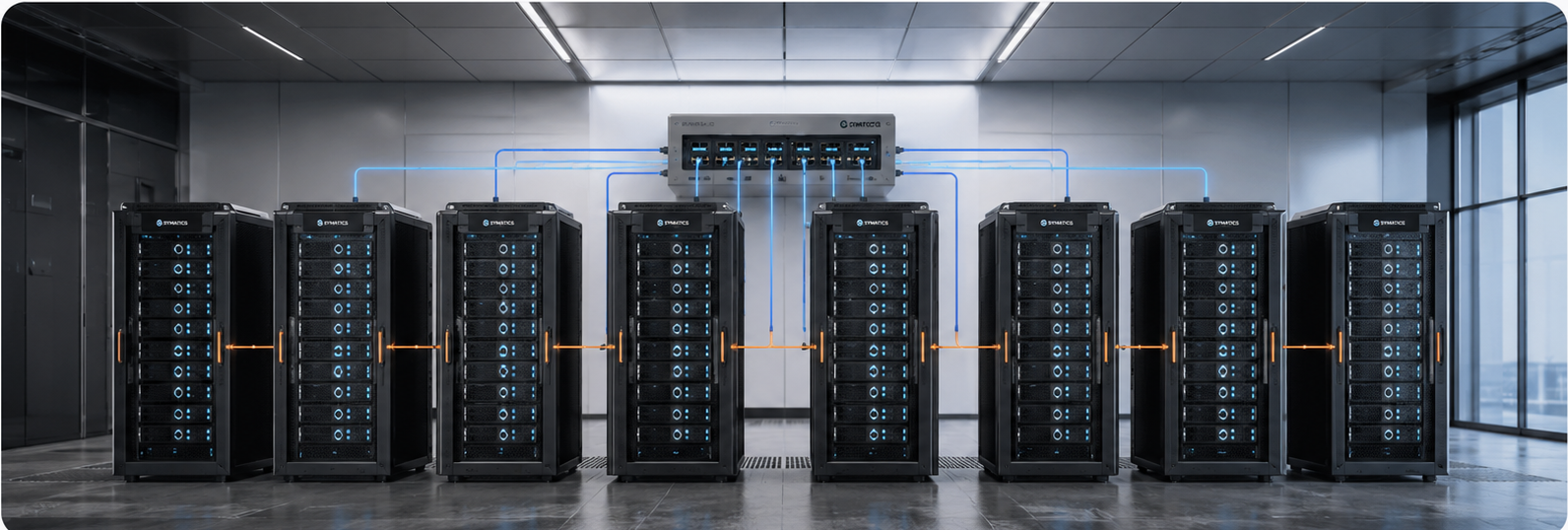
64-chip domain
A single domain converges to one 64-port hub die — one tape-out, no Spine/Root split.
| Component | Qty | Specification |
|---|---|---|
| MPU Chip (+ on-die SCC) | 64 | N7 ~430 mm²; ~250–350 W; 32,768 CUs each |
| CSL (Column State Loader) | 64 | One per chip; Gen1 Memory Ingress Block; eta ~45% |
| GDDR7 Devices | 256 (4/chip) | ~192 GB/s/chip; ~12.3 TB/s aggregate raw |
| SIF Switch Hub | 1 | 64-port; 256 lanes; ~390 mm²/N7; 1-hop < 200 ns |
| Host Node | 1 | Dispatch / serving / image load; no data-plane scheduling |
| BMC / Management | 1 set | I2C bus + telemetry aggregation + secure boot chain |
Single-Hub Dividend
The entire domain's switch silicon converges to one 64-port hub die (~390 mm²/N7), one tape-out, no Spine/Root split. Within the domain, a 1-hop <200 ns replaces the prior 6-level tree.
Evidence boundary: All chip parameters are analysis-derived from the CU-array architecture walkthrough, not silicon-measured. Die size, power, and SRAM feasibility have been cross-checked against published N7 data (e.g. Graphcore GC200 at 1.09 MB/mm² on the same node). Tape-out will validate.
64 chips. One hub. One hop.
A domain is the minimum deployable system unit: 64 MPUs + a single 64-port SIF hub + host node, physically about one rack. Every MPU reaches every other MPU in under 200 nanoseconds — through a single hop, not a multi-tier tree.
Three independent bandwidth channels
The domain has three bandwidth channels, each sized for its specific role — and they never borrow from each other.
Weight Ingress
DDR7 to CSL to column. The real decode wall. Every token re-reads active weights through this channel.
State Traverse
SIF single-hub broadcast. Only bounded intermediate state (~16 KB/token/edge) — roughly 1000x headroom.
Scale-Out
Inter-domain direct rails, no switch. For logical column extension. Copper, no SerDes needed.
What the SIF hub deletes
The MPU Switch is not a general-purpose switch. It carries only structured, compile-scheduled broadcast — no dynamic routing, no runtime arbitration, no GPU-style collectives. Everything a CXL or PCIe switch spends silicon on to manage unpredictable traffic is removed by design.
Deleted by construction
What remains
A flat 64-port hub with a stateless datapath: 64:1 source-select uplink + 1:64 broadcast downlink, 3 on-die pipeline stages. Per-row single-source broadcast across 128 groups. Fixed latency under 200 ns. No queues, no arbitration, no runtime decisions.
Scale-out: extend, don't stack
Two scale-out modes, zero new switching tiers. Adding domains is pure structural replication — no new protocol layers, no fat-trees, no new system complexity.
Structure Extension
Capacity Axis
Adjacent domains connect via direct peer rails — no switch, no SerDes, just copper. The logical column simply gets longer; the compiler sees a larger array. For when a single model doesn't fit in one domain.
Domain Replication
Throughput Axis
N independent domains run independent streams. Front-end dispatch over standard Ethernet. Throughput multiplies linearly. This is system simplicity, not efficiency magic — cost and power scale proportionally.
SuperPod: 8 domains, one chain
At machine-room scale, 8 domains compose into a row-of-racks chain — physically adjacent, connected by direct peer rails. Three configurations from the same hardware: one super-array, 8 independent domains, or hybrid. Compile-time decides, not hardware SKUs.
Full Chain
One (8×64×256)×128 super logical array
Full Replication
8 independent domains × dispatch
Hybrid
2× 4-domain or 4× 2-domain chains